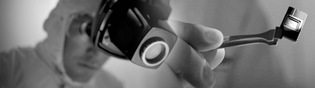
Integrated Nanosystems Research Facility


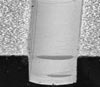
Devices made with Laurell Photoresist Spinner
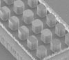
 MICROPALLET ARRAY
The micropallet array consists of hundreds of thousands of micro – scale pedestals, termed “micropallets” that are photolithographically patterned in an array on a 1”x3” glass coverslip. This technology will be used for the analysis of primary tumor cell subsets of clinical relevance at single cell resolution.
 METAL PLATING
Plating metal on non-conductive materials surface is widely used for fabricating compact electronic devices. A key difference between plating on non-conductive materials and plating on metal substrates is that the former requires a more highly specialized pretreatment to achieve the desired result.
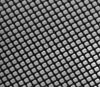
 SILICON MOLD
Si mold allows lower cost for mass manufacturing of PDMS microfluidics, easier cleaning and longer reusability of the Si master compared to conventional photoresist master.
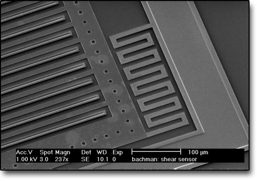 MICRO SHEAR STRESS SENSOR
SEM scan of a surface micromachined device designed at UCI to measure shear stress on wing surfaces during wind tunnel tests.
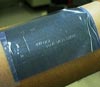 FLEXIBLE MICROFLUIDIC MEMBRANES
Demonstration of microfluidic channels system built using UCI technology (shown attached to human forearm).
 FLEXIBLE MICROFLUIDIC MEMBRANES
Demonstration of device to measure mass flow in natural gas engines. The piece is micromachined silicon, silicon nitride, and gold.
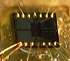
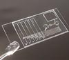 MICROFLUIDIC CHIP AASSAY DEVICE
Demonstration of device to measure mass flow in natural gas engines. The piece is micromachined silicon, silicon nitride, and gold.
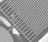
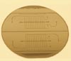 SU-8 MOLD
This is a fabricated SU-8 mold on a silicon wafer used to cast PDMS biochips to study cancer cells.