Integrated Nanosystems Research Facility


Highlights
Current INRF Newsletter
Read more
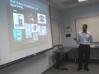 In summer 2016, INRF piloted a course series, Cleanroom Fabrication Processing Techniques through the CHAMP Program. Read more.
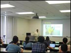 INRF/BiON hosted an intro course on cleanroom fundamentals, covering photolithography, dry/wet etching, microscopy and more. Read more.
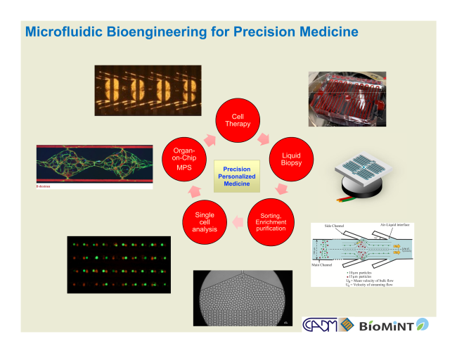
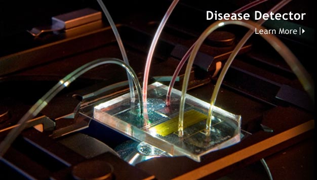
 INRF Faculty User and EECS Professor Peter Burke receives NIH NCI Award to develop a nanofluidic chip to ultimately learn more about why cancer cells respond to signals differently than non-cancerous cells. Read More.
 Professor Peter Burke honored with faculty innovator award.
 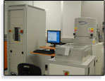 SPTS APS PM is an ICP-based high density plasma source, designed to etch materials which are difficult to etch using conventional RIE or ICP sources.
Learn More.
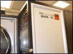 New equipment available at INRF.
Learn More.
New equipment available at INRF.
Learn More.

Engineering the Microworld
 The Integrated Nanosystems Research Facility at The University of California, Irvine (INRF UCI) in the Henry Samueli School of Engineering is dedicated to developing and promoting micro and nano technology through research, education and outreach. The INRF advances multidisciplinary research through fostering communication between traditionally distant fields such as bioscience and engineering and by enlisting researchers from diverse backgrounds. The facility is a 9,600 square foot class 100/1,000/10,000 clean room equipped with all the major devices for micro and nano fabrication. Capabilities include such diverse disciplines such as MEMS, biology, chemistry, optics and physics equipped with all the major devices for micro and nano fabrication.
Our facilities are available to our distinguished faculty and students along with other academic institutions and industry. We welcome you to visit us, take a tour and join us in performing high quality research at our world class facility to engineer the microworld.