Integrated Nanosystems Research Facility


INRF / BiON Devices
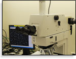
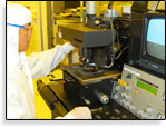
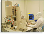
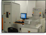
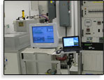
The INRF and BiON clean rooms utilize state of the art tools for performing manufacturing at very small size scales. Many of the techniques are borrowed from the semiconductor industry and adapted for making biomedical devices. The INRF/BiON facilities have unique tools for performing precision work in polymers, including wet lithography, laser etching, hot embossing, electroless metal deposition, surface modifications. In addition, our researchers have developed specialized materials and processes that are useful for micro biomedical devices, such as biocompatible photostructural polymers, protein patterning techniques, and laminate assembly.
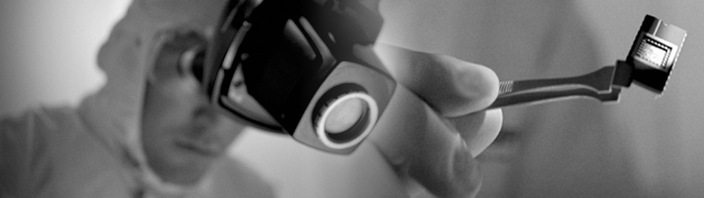
Below are examples of devices made in the INRF/BiON cleanrooms using our equipment.