Integrated Nanosystems Research Facility


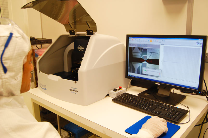
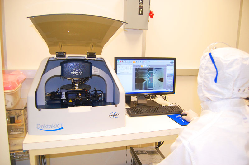
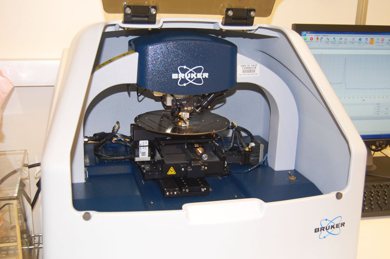
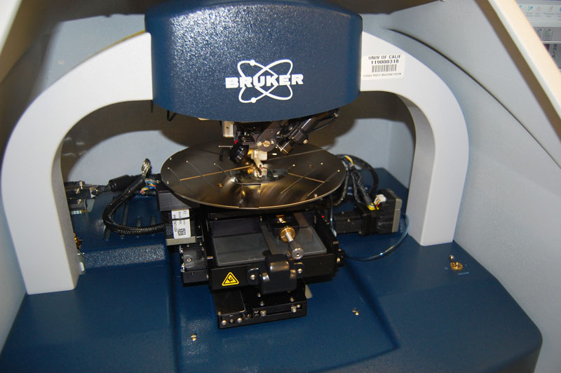
Dektak XT Profilometer

3D Mapping and Automation Packages
The Dektak XT can be configured with a 4-inch Y auto stage that enables 3D imaging. Or it can be equipped with a 6-inch X-Y auto stage that, in addition to 3D mapping, provides automation and programmability of over 200 sample sites.
Larger Samples and Longer Scans
The innovative design of the Dektak XT accommodates samples up to 3-inches thick, performs long scans of 55 millimeters, and provides a larger X-Y translation than competing systems. With the scan-stitching package, the system can perform even longer scans for stress measurements on larger wafers. Other stage features include wafer alignment pins for ease of use, three-point suspension for stress, lateral calibration for 99.9% accuracy, and a larger scan block for improved baseline stability.
Superior Repeatability
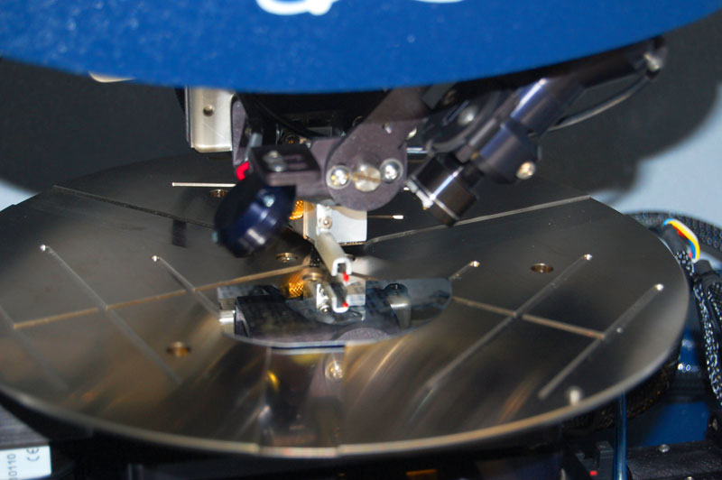
With 6-angstrom step-height repeatability, the Dektak XT profiler provides the flexibility to perform precise step-height measurements for thin films down to less than 100 angstroms, as well as thick-film measurements up to several hundred microns thick. The Low-Inertia Sensor 3 (LIS 3) head incorporates key technology advances to deliver extremely accurate measurements with unprecedented sensitivity.
Larger Vertical Range
The 512-micron vertical range is the best standard Z performance in the industry, and a 1-millimeter option extends the vertical range of these systems even further. The result of all these features is exceptional horizontal and vertical resolution, enabling precise planarity scans for measuring radius of curvature, flatness, and waviness, as well as characterizing thin-film stress on wafers.
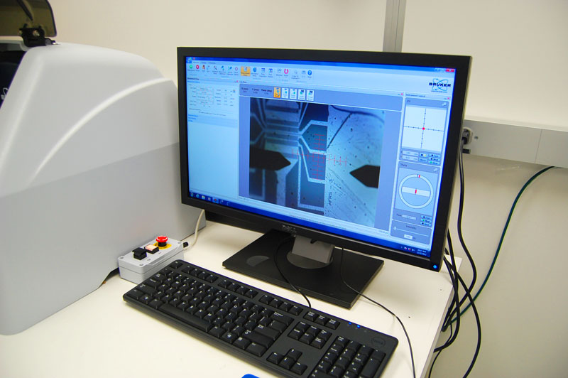
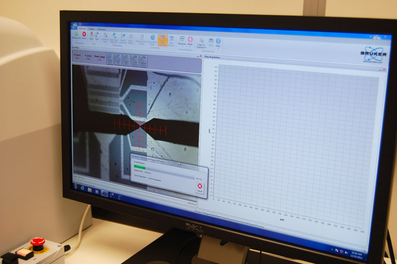
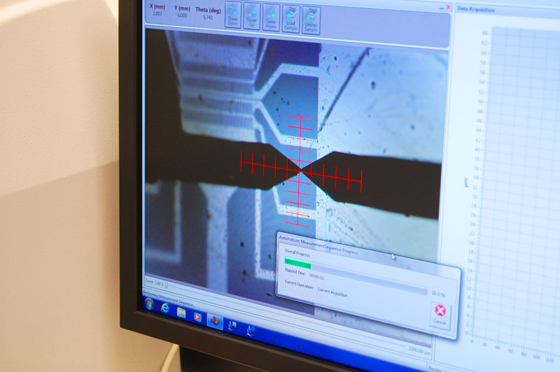
Powerful, Easy-To-Use Software
The software interface allows the operator to quickly become a Dektak expert. Analysis functions are both comprehensive and intuitive, from simple one-button load-and-go testing to automatic comparisons of analytical results from multiple scans. The Vision® analysis package further extends the usefulness of the Dektak XT data, enabling true 3D mapping, bearing ratio, and over 200 additional analyses.
Microform Measurements, Lowest Stylus Force
The new MicroForm™ package reveals difficult shapes and overcomes steep slopes, improving accuracy to within 0.25°. Similarly, the Low-Force option improves stylus sensitivity to 0.03 milligrams to enable non-destructive characterization of delicate surfaces. Plus, additional analysis capabilities have been added, such as histogram and advanced automation program summary for pass/fail analysis.
Customized For Your Applications
Whatever your application, we can configure a system to meet your specific requirements. Metal etch uniformity on wafers Thin-film stress calculations Transparent films/photoresist thickness, thin- and thick-film measurements Large-step MEMS characterization Microlens height/curvature and V-groove depth analyses Roughness studies on machined parts Aspheric lens characterization Surface quality and defect review High aspect ratio trench depth measurements And much, much more!