Integrated Nanosystems Research Facility


Dektak 3 Profilometer

Description
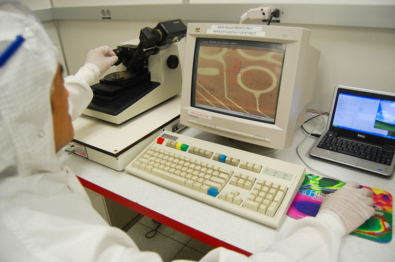
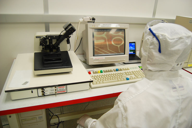
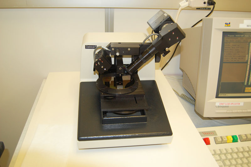
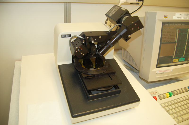
The Dektak 3 Surface Profilometer is an instrument to measure the vertical profile of samples, thin film thickness, and other topographical features, such as film roughness or wafer bowing.
A diamond stylus is moved vertically into in contact with the sample and then moved laterally across the sample for a specified distance and specified contact force. The instrument can measure small surface variations in vertical stylus displacement as a function of position. The Dektak profilometer can measure small vertical features ranging in height from 100 Å to 650,000 Å on a 5″ Diameter Sample Stage. The height position of the diamond stylus generates an analog signal which is converted into a digital signal stored, analyzed and displayed. The radius of diamond stylus is 12.5 microns, and the horizontal resolution is controlled by the scan speed and scan length. There is a horizontal broading factor which is a function of stylus radius and of step height. This broading factor is added to the horizontal dimensions of the steps. The stylus tracking force is factory-set to 50 milligrams.
General Information and Usage
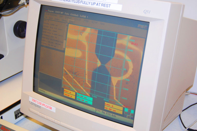
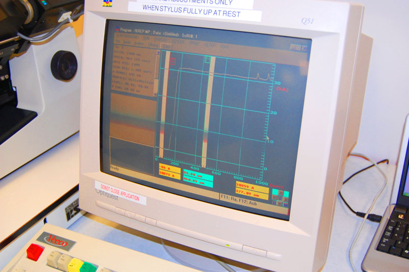
The Dektak is a profilometer for measuring step heights or trench depths on a surface. This is a surface contact measurement technique where a very low force stylus is dragged across a surface. The display range of the data is 200 Å to 655,000 Å (65.5 um) with a vertical resolution of ~ 5 Å. The lateral resolution is limited by the tip shape. A video camera with variable magnification allows for manual placement of the stylus and the system is programmed for scan length and speed. Data leveling is done in the software and printouts with cursor locations and step heights are provided. The data can also be saved to a PC for further analysis.
Functionality
The purpose of the DekTak is to give an engineer a quantifiable measurement of the surface profile of a wafer. This can be used to measure the height or width of a feature of the wafer surface, such as an etch, a metal deposit, or resist thickness. The profile can also give the engineer a look at the roughness of the surface of a wafer. The profilometer operates by lightly dragging a sharp stylus over the surface of the substrate and recording the vertical profile of the surface.
Technical Specifications
| Vertical Range: | 100Å to 1,310KÅ (0.4 microinch to 5mils) |
| Vertical Resolution: | 1A/65KÅ, 10Ål655KÅ, 20Åt1310KÅ |
| Scan Length Range: | 50 microns to 50mm (2 mils to 2 inches) |
| Scan Speed Ranges: | Low, Medium, High |
| Scan Time Range: | 3 seconds to 50 seconds |
| Software Leveling: | Two-point programmable or cursor leveling |
| Stage Leveling: | Manual |
| Stylus (standard): | Diamond, 2.5 micron radius |
| Stylus Tracking Force: | Programmable, 1-40mg (0.0 1-0.4mN -milliN ewtons) |
| Maximum Sample Thickness: | 45mm (1.75 inches) |
| Sample Stage Diameter: | 165mm (6.5 inches) |
| Sample Stage Translation: | X Axis ±76mm (±3 inches) |
| Sample Stage Translation (from center): | Y Axis -76mm (-3 inches) |
| Maximum Sample Weight: | 0.5Kg (lib) |
| Power Requirements: | 100/115/200Vac ±10%, 50-60Hz, 200Vac |
| Warm-up time: | 15min recommended for maximum stability |
| Operating Temperature: | 21°C ± 30C / 70°F ± 5°F |
| Zoom Magnification: | 35x to 200x |
| Camera: | Solid state monochrome video image |
| Sample Illumination: | Variable intensity white light; IR & UV blocked |
| Dimensions (Scan Head wIMonitor): | 33cm W x 56cmD x 81cmH |