Integrated Nanosystems Research Facility


Newsletter Issue 8
March 30 | Issue 8
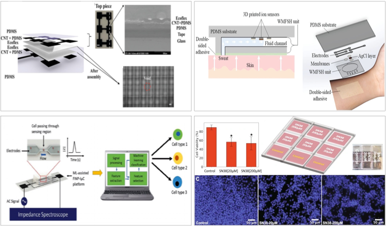
Faculty Spotlight – Rahim Esfandyarpour
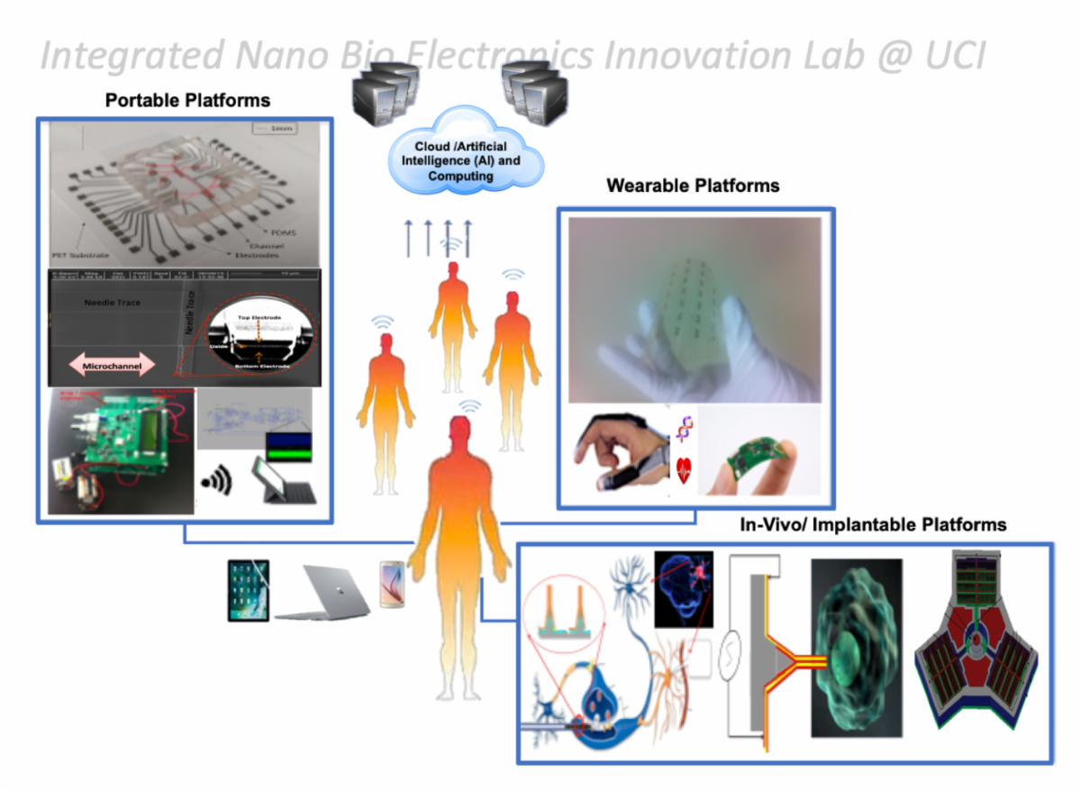
We present this month a member of the INRF research community, Rahim Esfandyarpour. Esfandyarpour received his Ph.D. and M.Sc. in Electrical Engineering from Stanford University. He is currently an assistant professor of electrical engineering & computer sciences and biomedical engineering. His interdisciplinary research group focuses on applying innovative engineering concepts to address major challenges in modern life science and medicine. They design, model, micro/nanofabricate, and validate innovative, state-of-the-art, novel -omics, and multi-level Next-Generation Smart (NGS) Wearable & Portable NanoBioElectronic devices to truly mimic an individual’s overall dynamic health. Toward this goal, his group aims to integrate innovative micro/nanoelectronics and functional nanomaterials using novel next-generation manufacturing technologies, supported by intelligent computing techniques (e.g., ML), along with smart electronic system designs. In his lab, students combine expertise in micro/nanoelectronics, flexible and wearable electronics, micro/nanofabrication, micro/nanotechnology, micro/nanoelectromechanical (N/MEMS) systems, micro/nanofluidics, nanomaterials, 3D-bioprinting, and microelectronic circuits and systems design.
Equipment Spotlight
Karl Suss MA6 Mask Aligner
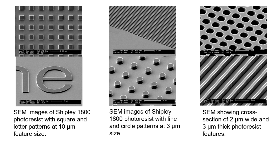
Karl Suss MA6 is a double-sided contact mask aligner and can be used to perform high-resolution photolithography. The tool is a mask alignment and exposure system that works for 4″ wafers and 5″ masks with positive photoresist lithography. Smaller wafers and chips may be mounted to a 4″ carrier wafer and processed.
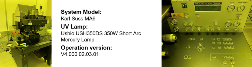
Specifications
- Light source: broadband covering 436, 405 and 365 nm
- Contact mode: hard contact, soft contact, vacuum, proximity, flood exposure
- Alignment: top side and bottom side
- Exposure intensity: 7.5 mW/cm2 (channel #1) and 10 mW/cm2 (channel #2)
- Exposure uniformity: ± 5% across 4”
- Maximum wafer size: 4”
- Mask size: 5” x 5”
- Top side microscope travel range: X: ± 25mm; Y: -75~+25mm
- Bottom side microscope travel range: X: 0~30mm; Y: 0~70mm
- Wafer stage travel range: X: ± 10mm; Y: ± 5mm; theta rotation: ±5°
- Minimum feature size: 2 µm (with hard mask); 10 µm (with soft mask)
- Alignment accuracy: 2 µm
- Spin coater, developer bench, optical microscope, SEM, and Dektak profilometer on site for easy inspection and characterization
Results