Integrated Nanosystems Research Facility


Newsletter Issue 6
September 16 | Issue 6
Welcome to the new INRF monthly newsletter where we will be sharing equipment capabilities, updates and research accomplishments.
Industry Partner Spotlight – Carbon Technology Inc.
We would like to introduce one of our industry users, Carbon Technology, Inc.
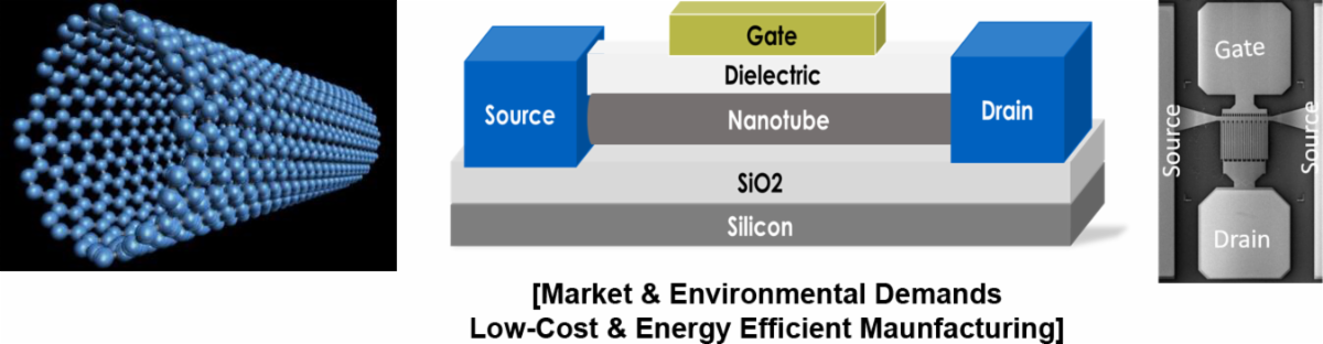
Carbon Technology, Inc. is developing next generation semiconductor solutions based on carbon nanotubes. The superior properties of carbon nanotube devices will spur their adoption dramatically, improving the trade-off between speed and power while delivering unprecedented robustness.
Carbon nanotubes are a single layer or multiple layers of carbon sheets formed into a cylinder or “nanotube.” Single walled carbon nanotubes (CNTs) naturally range from 0.8 to 3 nanometers in diameter with one-third being metallic. CTI (Carbon Tech) has developed methods to grow just semiconducting tubes with the diameter needed for high performance electronics.
The electrical and thermal properties of semiconducting carbon nanotubes make them among the best bets to replace current bulk semiconductors. Electron transit along the tube’s axis shows 50x the mobility (how fast an electron moves with voltage) of silicon electrons and 200x that of silicon holes. For RF, the electronic structure of CNTs results in inherently linear amplifiers. Carbon nanotubes also exhibit superb robustness to heat and radiation.
Carbon Nanotube Field Effect Transistors (CNTFETs) need to start with the right material and add robust, low resistance contacts and the right protection to keep everything clean. CTI has demonstrated each of these key elements and the high yield manufacturing needed to produce in volume.
Research and Development
The INRF has been key to CTI’s development work to date. UCI Ph.D. and Carbon Tech founder and CTO Dawei Wang did his PhD research in the INRF. After his thesis defense, he continued working in the INRF for RF Nano Corporation where he produced the first GHz nanotube transistors. Building on this success, a highly uniform production flow for carbon nanotube-based field effect transistors was developed in the INRF. The work at Carbon Tech has been focused on improving nanotube materials needed for commercial grade parts. This is the unsolved problem that has kept this remarkable material from delivering against their promise. The same was true for gallium arsenide (GaAs) which was largely understood in the 1960s but required another 30+ years of materials development before GaAs played its integral role in transforming the car phone into the cell phone. This difference between nanotubes and GaAs makes the difference between GaAs and silicon look pedestrian.
This month we are highlighting the
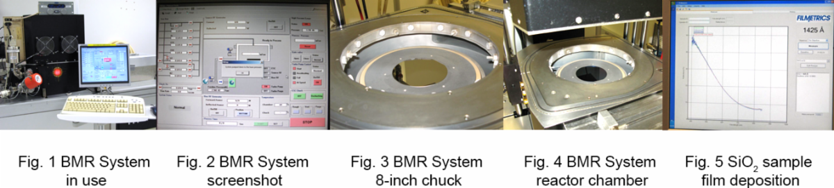
BMR HiDep PECVD System
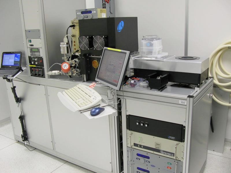
The BMR HiDep System is a inductively coupled plasma enhanced chemical vapor deposition (ICP-PECVD) tool, it consists of a single wafer (up to 8-inch) process reactor chamber, and has the following gases for processing: CF4, Ar, SiH4, O2, N2, H2, and CH4.
The highly dissociated plasma of BMR HiDep significantly lowers the required process temperature for excellent quality dielectric films deposited at 200°C or lower such as Silicon Dioxide (SiOs), Silicon Nitride (Si3N4), Amorphous Silicon (a-Si), Silicon Carbide (SiC), and Diamond Like Carbon (DLC).
This capability enables dielectric film deposition on temperature sensitive materials.
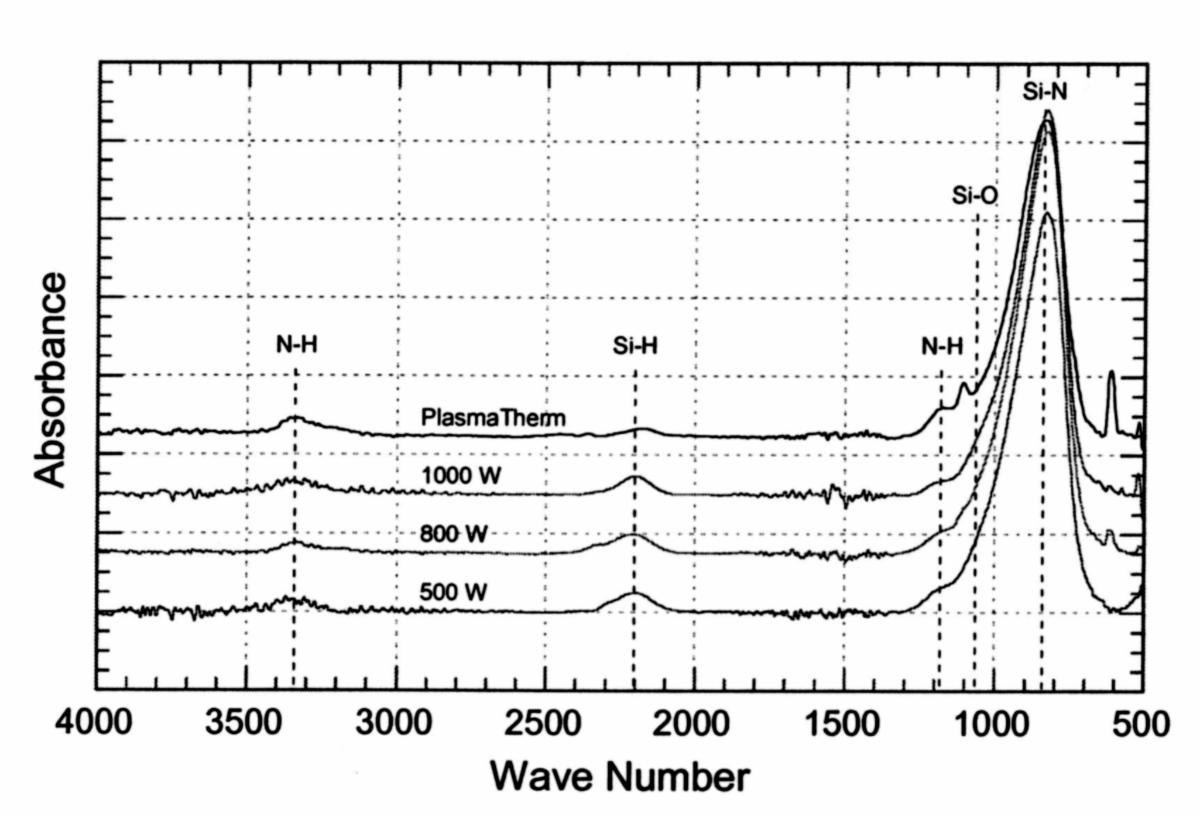
Silicon nitride is one of the most widely used thin film dielectrics in a broad range of microelectronic, photovoltaic, and photonic devices. In addition to its remarkable electrical properties, silicon nitride has high chemical and thermal stability, satisfactory optical transparency, remarkable moisture resistivity, and good mechanical strength as shown in the figures.
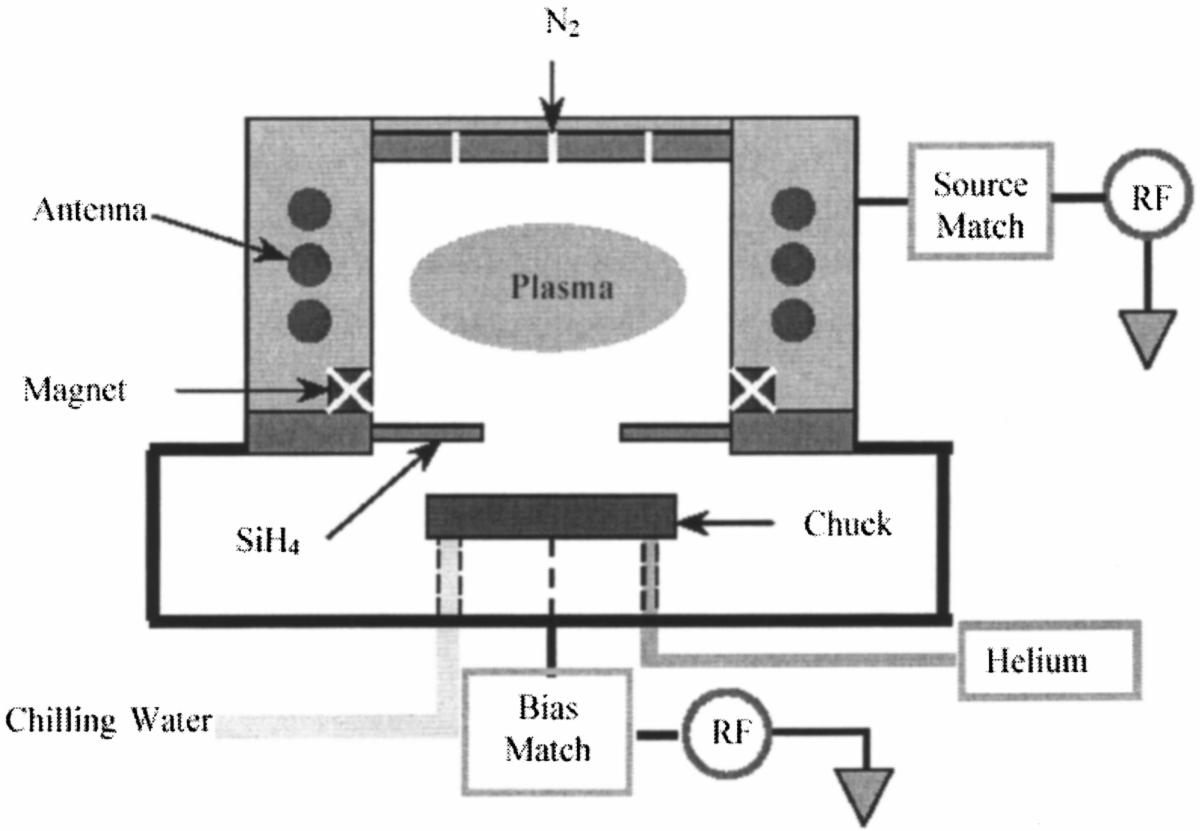
Schematic diagram of the ICP-CVD reactor.
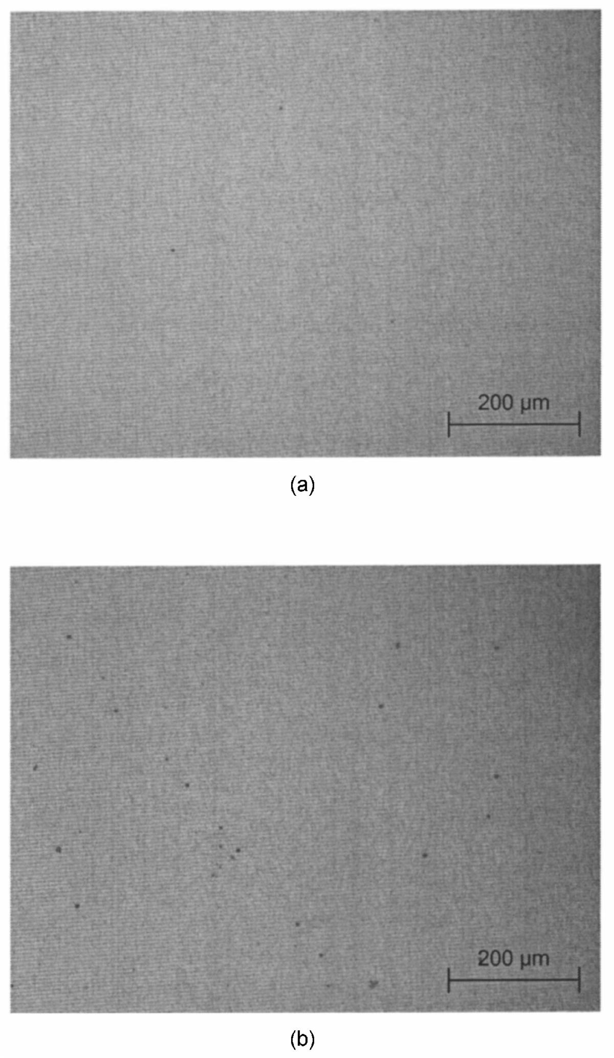
Pin holes are common microstructural defects of thin dielectric films made by any chemical or physical vapor deposition technique. Pin holes density evaluation, shown here, by KOH etching at 70C for 3 hours.