Integrated Nanosystems Research Facility


Newsletter Issue 5
July 1 | Issue 5
Welcome to the new INRF monthly newsletter where we will be sharing equipment capabilities, updates and research accomplishments.
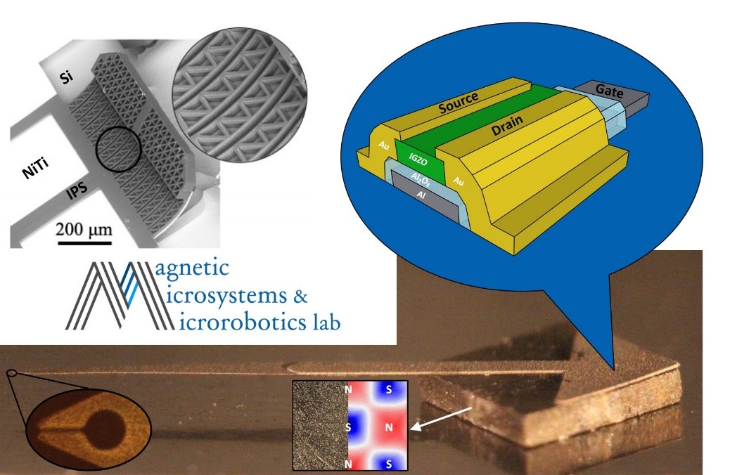
Faculty Spotlight – Camilo Velez Cuervo

We present this month a new member of the INRF research community, Camilo Velez Cuervo. Camilo is an assistant professor of Mechanical and Aerospace Engineering. He received his Ph.D. and M.Sc. in electrical and computer engineering at University of Florida, a M.Eng. at Universidad de los Andes-Colombia, and his B.S. in electronic engineering at Pontificia Universidad Javeriana-Colombia. He was a postdoctoral researcher at Carnegie Mellon University in the Microrobotics Lab and at the Interdisciplinary Microsystems Group at University of Florida. He currently serves in the board of Governors of Electron Devices Society at IEEE, as chair of Young Professionals committee, and member of Microelectromechanical Systems in the same society.
Research and Development
His laboratory’s dream is to create a swarm of functional robots, the size of a cell, working together to solve complex problems by themselves. Those microrobot units must be made smaller, smarter, cheaper, and more capable than anything seen before. To fully realize this futuristic vision, Camilo has created the Magnetic Microsystems & Microrobotics Lab, with the research goal of increased micro robot autonomy and functionality to solve medical, industrial and manufacturing problems. Students at this lab combine expertise in microrobotics, microfabrication, MEMS, patterning of magnetic materials, microfluidics and semiconductor devices.
This month we are highlighting our
Denton DV-502M Sputter System
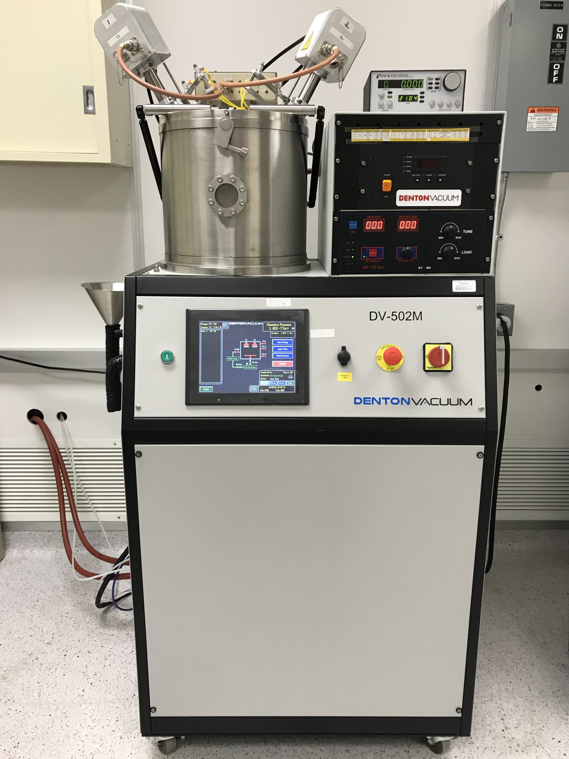
System Model:
Denton DV-502M
Sputter Source:
Sierra Applied Sciences (SAS) Planar Magnetron Sputter Cathodes
Deposition Thickness Monitor:
Inficon SQM-160
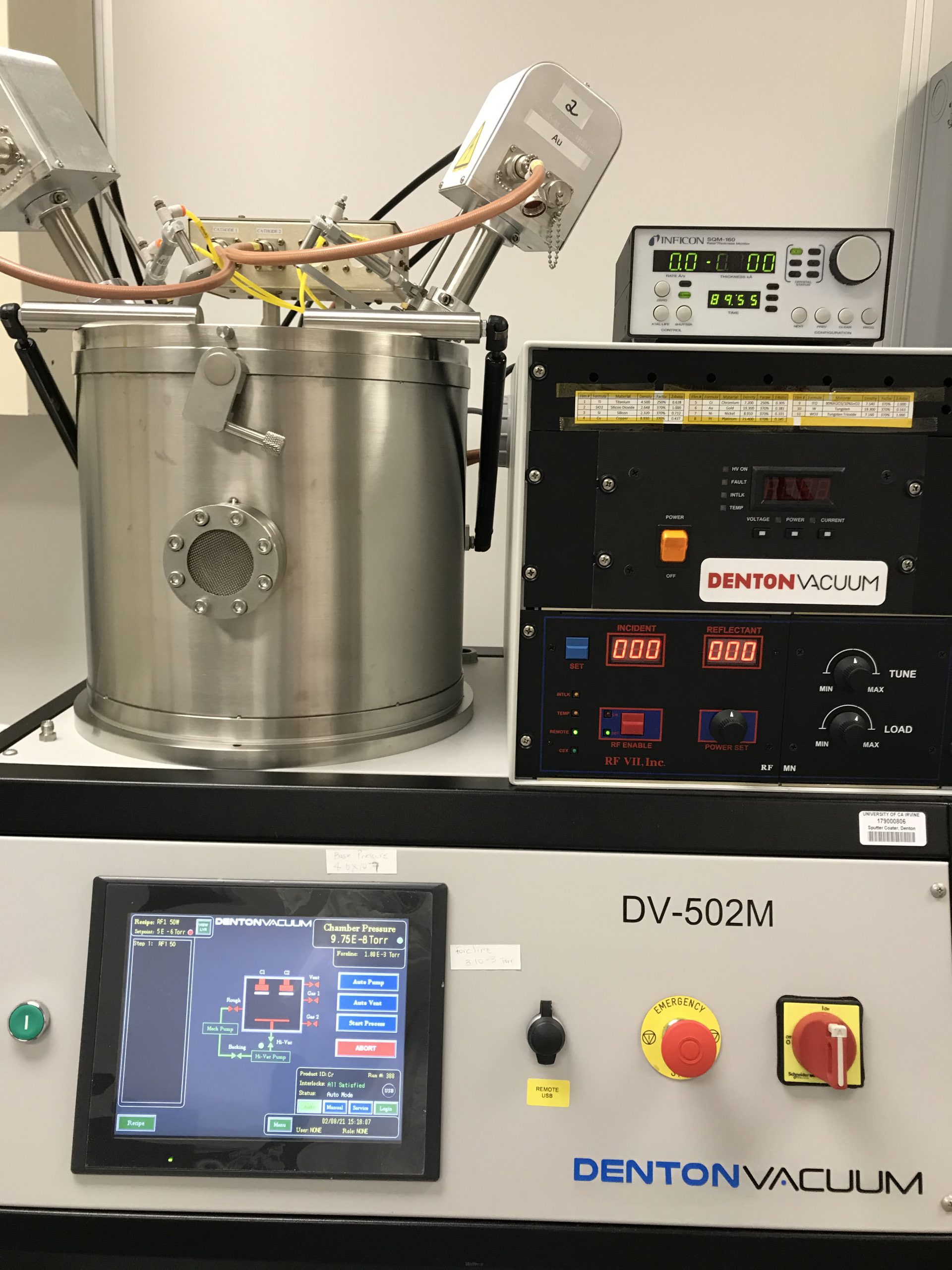
Specifications
- Equipped with two confocal water cooled cathodes using standard 2″ targets
- DC and RF power supplies can be switched between both cathodes
- Maximum RF power: 300 W
- Maximum DC power: 600 W
- Substrate stage rotation speed: 0-20 rpm
- Substrate stage size: 4″
- Argon MFC flow rate: 0-200 sccm
- Reactive sputtering capability with oxygen needle valve control
- Fast pumping down speed (30 minutes to 5E-6 torr) with turbo pump
- Deposit metal, semiconductor, and dielectric (with SiO2, Au, Pt, Cu, Cr, Ti targets in-house)
- Thickness uniformity: +/- 5% across 4″ wafer
- Touch panel graphical interface to the PLC with automatic process control
Sample Results
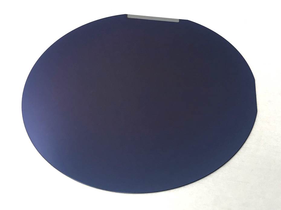
Optical image of target 1000 angstrom silicon oxide deposited on 4″ silicon wafer with RF sputtering from Cathode #2. Deposited film was measured with ellipsometer to be 1017 angstrom +/- 3%.
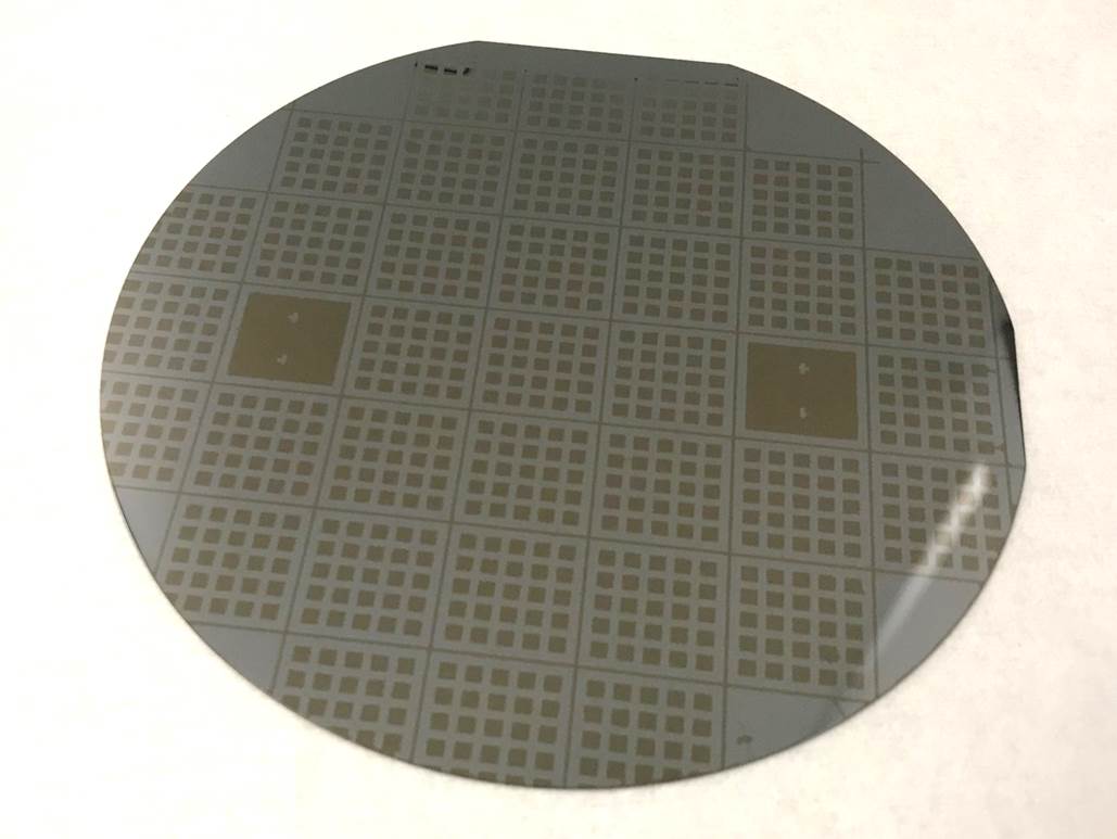
Optical image of titanium deposited and patterned on 4″ silicon wafer with DC sputtering from Cathode #!. Deposited film was measured with Dektak XT profilometer to be 1800 anstrom +/- 3%.
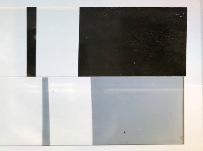
Tungsten oxide was deposited with reactive sputtering from tungsten target and reactive oxygen gas. Optical images showed opaque tungsten (without O2 gas) and transparent tungsten oxide (with O2 gas) sputtered on glass.