Integrated Nanosystems Research Facility


Newsletter Issue 4
June 2 | Issue 4
Welcome to the new INRF monthly newsletter where we will be sharing equipment capabilities, updates and research accomplishments.
Faculty Spotlight – Javier Sanchez Yamagishi

This month we spotlight a member of the INRF research community, Javier Sanchez-Yamagishi. Javier Sanchez-Yamagishi is an Assistant Professor in the Department of Physics & Astronomy at the University of California, Irvine (since 2018). His lab studies quantum electronic transport in 2D and topological materials with an emphasis on developing fabrication and measurement techniques. Previously, he was a postdoctoral fellow at the Harvard Quantum Optics Center where he explored the application of spin qubits as nanoscale magnetometers for 2D materials. For his PhD work at MIT, he studied the electronic properties of twisted graphene heterostructures.
Research and Development
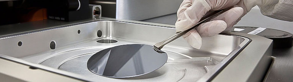
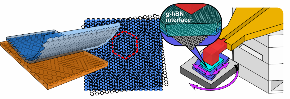
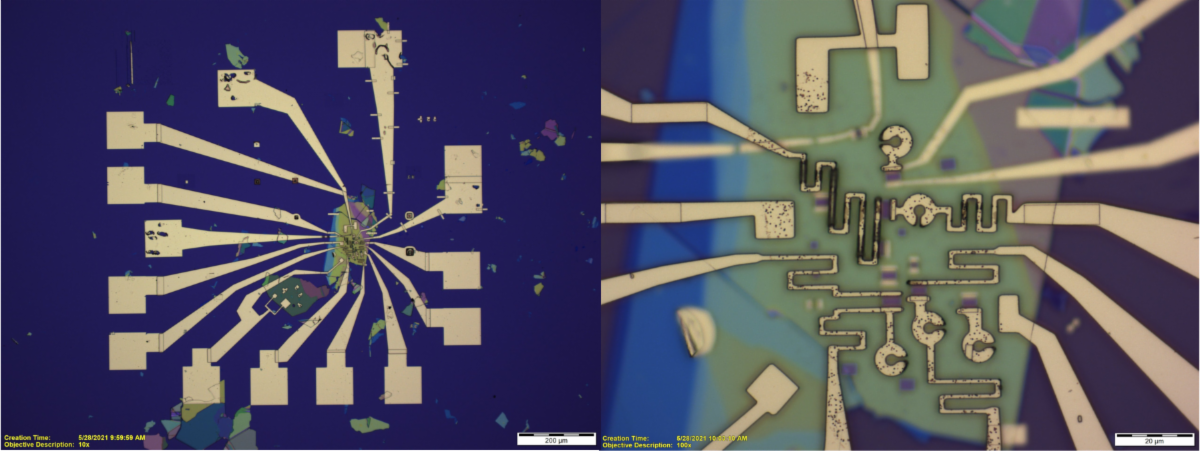
Currently, the Sanchez-Yamagishi group is developing new techniques to manipulate heterostructures of 2-dimensional van der Waals materials. Such materials like the single-atom thick graphene can exhibit exotic electronic properties that depend sensitively on the relative crystal alignment between stacked crystals. The research team has developed techniques to dynamically modify in-situ the physical structure of 2d material devices. This is enabled by the low friction sliding between van der Waals bonded crystals. The team is applying these dynamic structural control techniques to (1) investigate dynamic electronic effects that arise from sliding moiré superlattices, and (2) systematically study correlated and topological physics of multi-moiré systems by in-situ control of twist angle and layer displacement.
This month we are highlighting our
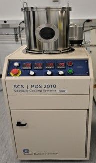
PDS 2010 Parylene Deposition System
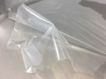
 | Parylene C Parylene C, the second commercially available member of the Parylene series, is produced from the same raw material (dimer) as Parylene N, modified only by the substitution of a chlorine atom for one of the aromatic hydrogens. Parylene C has a useful combination of electrical and physical properties, plus a very low permeability to moisture and corrosive gases. | 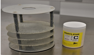 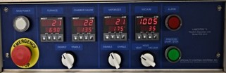 |

Richard Chang, Senior Process Engineer
The PDS 2010 is a vacuum system used for the vapor deposition of the Parylene polymer onto a variety of substrate. The clear polymer coating formed provides an extremely effective chemical and moisture barrier with high dielectric and mechanical strength. If you have any interest in using the Parylene system please contact
Richard Chang at the INRF. Richard Chang has over 20 years of experience working within the INRF for micro-fabrication. He is the one of the key trainers in INRF with the photolithography, thin film deposition, chemical cleaning, wet etching, dry etching, characterization analytical tools, and so on. His expertise is in micro-fluidic and micro-pallet device fabrication.
Tool Specifications:
Controls , computerized sequencing using microprocessor temperature and process controllers. Automatic and semi-automatic operation with fault condition and end-of-run monitoring for controlled shutdown sequence.
Dimer capacity: 125 grams
The cold trap by: Liquid Nitrogen Substrate Material: Silicon wafer, metal, plastic, elastomer, glass, paper, etc.,
Substrate size: around 3 piece of 4 inch Silicon wafers
The adhesion: A-174 silane
The loading fixture: 3 layers
Sample Results
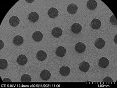
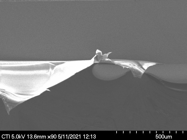
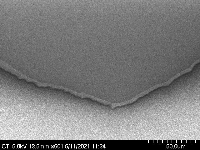
SEM of Deposited 5 um Parylene C and Plasma etched pattern
Deposited 5 um Parylene C film


Parylene C deposition rate:
5um/ hour or 0.5um/ Gram