Integrated Nanosystems Research Facility


Newsletter Issue 1
February 28 | Issue 1
Welcome to the new INRF monthly newsletter where we will be sharing equipment capabilities, updates and research accomplishments.
Faculty Spotlight – Howard (Ho Wai) Lee
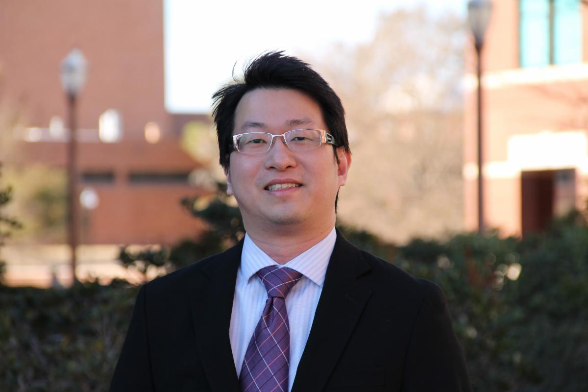
This month we spotlight a new member of the INRF research community, Howard (Ho Wai) Lee. Lee, a UC Irvine associate professor in the Department of Physics and Astronomy, also is affiliated with UCI’s Beckman Laser Institute & Medical Clinic. Before joining UCI in July 2020, Lee, who earned his doctorate in 2012 in physics from Germany’s Max Planck Institute for the Science of Light, was an associate professor in the Department of Physics at Baylor University, and a fellow and visiting professor in the Institute for Quantum Science and Engineering at Texas A&M. From 2012 to 2015, he was a postdoctoral fellow at Caltech, working with Prof. Harry Atwater in active plasmonics/metasurfaces. His current research focuses on active linear, nonlinear and quantum plasmonic/metasurface/zero-index optics, quantum biophotonics and imaging, “meta”-fiber optics and hybrid photonic-plasmonic on-chip optical devices.
From Dr. Lee,
My group studies extreme light-matter interaction, advanced nanophysics/optical materials and ultrafast/quantum/bio-photonics at the nanometer scale.
As affiliated faculty at Beckman Laser Institute & Medical Clinic and also part of the Convergence Optical Sciences Initiative (COSI), we are interested in using emerging nanophotonic platforms and “meta”-optical fibers for advancing optical imaging, sensing and medical applications. These include advanced in-fiber imaging endoscopy or laser surgery elements, tip-enhanced Raman spectroscopy for molecule detection and biosensing, novel optical fiber laser sources/nano-lasers and optical cooling/trapping platforms.
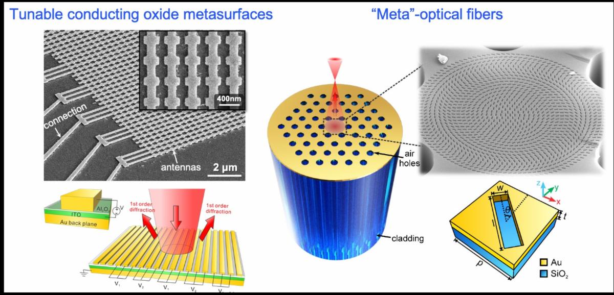
Our research involves developing advanced ultrathin nanophotonic structures and emerging active optical materials using the world-class nanofabrication facilities available at INRF. One project investigates ultrathin optical films, called optical metasurfaces, which are really thin: 1,000 times thinner than the width of a human hair. This metasurface can shape light for different functions; it can absorb almost 100 percent of the light that falls on it, focus light as a conventional lens and filter out specific colors − wavelengths of light − in the visible and invisible regions of the electromagnetic spectrum. These ultrathin metasurfaces could dramatically reduce the size and weight of a vast range of optical and electro-optical devices, while also improving their performance for energy, imaging/display, sensing and space technologies.
Another project involves the extreme optics of “zero refractive index” materials. Normally, materials have certain refractive indexes of light (for example, glass’s refractive index is ~ 1.5). But we can fabricate optical thin film that exhibits “zero” refractive index. These extreme materials show unique and abnormal optical features that are completely different from normal materials, including ultrafast nonlinearity, quantum properties and light emission properties that could lead to significant breakthroughs for developing ultrafast and ultracompact nanophotonic imaging, sensing and communication applications.
Our group also combines these advanced nano-optical structures into optical fiber to develop “meta”-optical fibers capable of advanced sensing, imaging and medical applications such as optical fiber endoscopes, in-fiber lasers for surgery and quantum bio-sensors.
This month we are highlighting our
FEI SEM and E-Beam Writing System
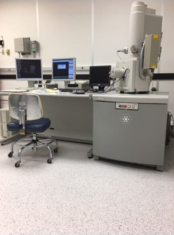
SEM Model:
FEI Sirion XL-30 FEG SEM
E-beam Writing System:
J.C. Nabity Nanometer PatternGeneration System (NPGS) v.9
Pattern Design Software:
DesignCAD LT

| Chuangyuan “CY” Lee, Senior Process Engineer |
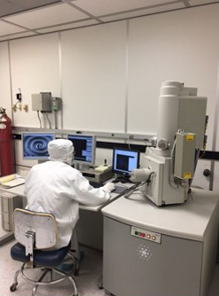
| The FEI Sirion XL-30 is a field emission gun (FEG) scanning electron microscope (SEM) system that can produce high resolution images and can also be used for small-area electron beam lithography. If you have any questions or interest in using this equipment please contact CY at the INRF. CY recently joined the INRF coming from Advantest America where he led a team to develop and manufacture advanced probe cards for the semiconductor industry. CY recevied his Ph.D. in Electrical Engineering from the University of Southern California and his B.S. in Electrical Engineering from the National Taiwan University. |
Tool Specifications:
SEM Microscope
-Motorized stage in 4 axis: X, Y, Z, Rotation (R)
-X/Y travel range: 50x50mm (+/- 25mm)
-Tilt range: -15 to +75 degrees
-CCD detector available inside SEM chamber
-Denton Sputter adjacent to FEI for metal coatingfor non-conductive specimens(semiconductor, polymer, biological materials)
Tool Specifications:
E-Beam Writing
-Resolution and field size
~50nm resolution with 100 um field @1000x
~100nm resolution with 200 um field @ 500x
~0.5um resolution with 500 um field @ 180x
~1 um resolution with 1mm field @ 90x
-Pattern design tool: DesignCAD LT software onNPGS computer. Also capable of DWG and DXFfiles (e.g. from AutoCAD) import to DesignCAD LT
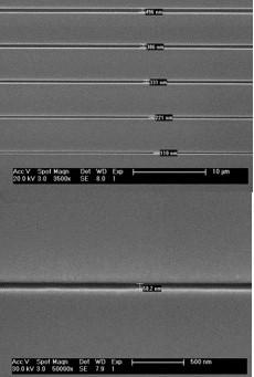
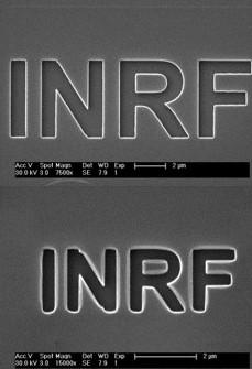
Sample Results
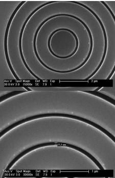
Different concentric circles were designed with DesignCAD LT and written with NPGS.
Lines with different sizes were patterned. 50nm line in design was patterned to be around 50.2nm.
1um feature size “INRF” designed on AutoCAD software, was imported to DesignCAD. A smaller (1/3) pattern was also created with Scale function.